Sonoki,
Both input differentia pairs are trimmed to zero at the wafer level but the die packaging-related stress causes a random Vos shift in both (a) and (c) modes. Mode (b) is a 400mV Vcm transition between P and N input differential pair being active where Vos moves gradually from P-channel Vos to N-channel Vos or vice-versa – see below for more details.
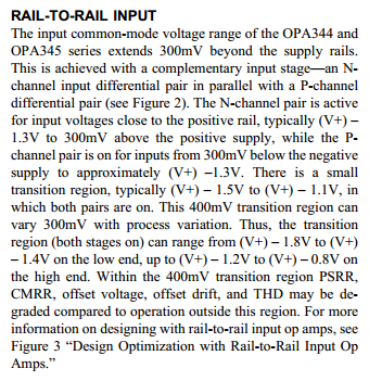
P-channel Vos , mode (a), is specified in PDS as typical of 200uV (one-sigma) and maximum +/-1mV – see histogram below.
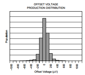
Since the random Vos change between P and N input pairs dominates the Common Mode Rejection Ratio spec, the expected Vos for N-channel Vos may be back-calculated from the CMRR spec shown below. For example, for Vs=5.5V, -0.3V<Vcm<5.8V, typical CMRR is 84dB (63uV/V) while the maximum CMRR is 70dB (316uV/V); thus the typical Vos change between (a) and (c) is: [(5.8V-(-0.3V)]*63uV/V=6.1V*63uV/V=384uV (twice the typ Vos in PCH) while the maximum Vos change is: 6.1V*316uV/V=1928uV (twice the max Vos in PCH); of course, they both may have positive or negative polarity.
From the above calculations you may see that the typical and maximum Vos shift as the input common-mode transition from (a) to (c) mode, or vice versa, is around twice the Vos specified for P-channel input differential pair so the expected distribution of Vos for N-channel (c) must be similar as for P-channel: typical 200uV and maximum 1mV. However, the two input offsets are completely random so there is no correlation between the two pairs - that means that, for example, PCH Vos of +200uV may typically transition to NCH Vos of +600uV or -200uV(200uV +/-400uV); therefore, it is critical to understand that the magnitude or polarity of the input voltage offsets in PCH input differential pair (a) does NOT relate in any way ANY information about the magnitude or polarity of Vos in NCH input pair even though both, (a) and (b), Offset Voltage distributions look very much similar like the one shown above.